News Category
USA-Japan Semiconductor Packaging Consortium "US‑JOINT" Begins Operations in Silicon Valley
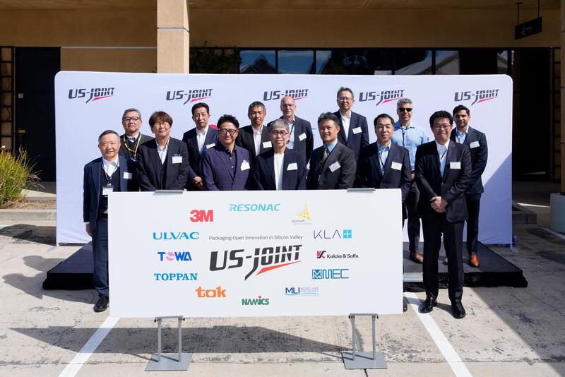
Union City, California―April 20, 2026―ULVAC, Inc. announced that US‑JOINT, a consortium comprising 12 Japanese and U.S. materials and equipment companies, has commenced full‑scale operations with the aim of establishing a new technology development model in the field of next‑generation semiconductor packaging. To mark the launch, an opening ceremony was held on April 20 (local time) at the consortium's site in Silicon Valley, attended by government representatives from Japan and the United States as well as representatives of participating companies.
US‑JOINT is the first consortium in the United States dedicated to the development of advanced semiconductor packaging technologies. Through the consortium, ULVAC hopes to contribute its expertise in vacuum technology via its plasma ashing and seed sputtering systems and their process technologies.
In growth areas such as generative AI and autonomous driving, rising semiconductor performance requirements are increasing the importance of advanced semiconductor packaging technologies. At the same time, despite the rapid emergence of new packaging concepts, limited opportunities for fast and practical validation have become a bottleneck in technology development.
US‑JOINT uses its research and development site in Silicon Valley to evaluate advanced semiconductor packaging concepts together with key customers. By combining the technologies of leading Japanese and U.S. materials and equipment manufacturers with an environment where semiconductor users and new ideas are concentrated in the United States, the consortium seeks to accelerate R&D in materials, evaluation, and implementation technologies and support the early practical application and commercialization of new technologies.
About US‑JOINT
| Name | US‑JOINT (JOINT: Jisso Open Innovation Network of Tops) |
|---|---|
| Purpose | Establishment of an evaluation platform for next‑generation semiconductor packaging and development of implementation technologies in the United States |
| Participating Companies | 12 companies (as of April 20, 2026) Azimuth Industrial, KLA Corporation, Kulicke and Soffa Industries, MEC Co., Ltd., Moses Lake Industries, Namics Corporation, TOKYO OHKA KOGYO CO., LTD., TOPPAN Inc., TOWA Corporation, ULVAC, Inc., 3M Company, Resonac Corporation |
| Location | Union City, California, USA |
| Start of Operations | April 2026 (full‑scale operation) |
| Key Facilities | Advanced semiconductor packaging processes (patterning, bonding, molding, plating, etc.), evaluation and analysis equipment, cleanrooms (Class 100 / 1,000) |
| Role of the Facility | R&D center for concept verification of next‑generation semiconductor packaging |
| Expected Users | Fabless companies, semiconductor manufacturers, and engineers from participating companies |
![]()
US‑JOINT Logo
For Further Information
ULVAC, Inc. elec_info