News Category
ULVAC Launches Dry Etching System "NA-1500" for 600mm Advanced Packaging Substrates --- NA-1500 provides uniform Descum process for large square substrate
ULVAC, Inc. (Headquarters: Chigasaki, Kanagawa; President and CEO: Hisaharu Obinata; hereinafter referred to as ULVAC) has developed a dry etching system for Descum processes and applicable to 600mm advanced packaging substrates.
Background
High-density packaging technologies using wiring pattern miniaturization, circuit resistance reduction and parasitic capacity removal have received attention in order to improve higher data transfer speeds amid the expansion of smart mobile device market and proliferation of "big data".
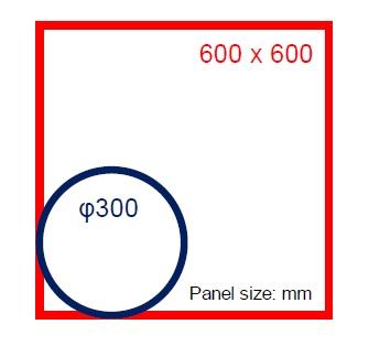
Therefore, advanced and thinner mobile devices such as smartphones are requiring thinner and higher-pin-count IC packages. To meet these demands, Fan-Out Wafer Level Package (FO-WLP) technologies have attracted attention, and mass production has started since last year. As the next step, packaging manufacturers have increased substrate size (Panel Level Package) from φ300mm to 600mm to quintuple the area ratio to significantly reduce FO-WLP production cost.
Although there are many dry etching systems for φ 200mm or φ 300mm wafers on the market, there has been no dry etching system for 600mm substrates which provides uniform Descum process*1 and Ti etching process. ULVAC has developed a new dry etching system to address this need and support the mass-produced packaging process.
Outline of the technology
ULVAC has sold more than 200 dry etching systems, mainly for φ300mm wafer used for Wafer Level Chip Size Package (WLCSP) over 20 years ever since we released the systems for φ200mm wafer.
Recently, we have developed the dry etching system for 600mm substrate by enhancing the proven plasma source. Our plasma source enables fast and low-temperature etching of resin layer that was impossible with the existing CCP*2 method. This plasma source is applicable to fluorine gases so that seed layer Ti etching, which requires wet process, can be removed without side etching. Furthermore, SiO2 and SiN etching are available.
Although warpage due to enlarged substrate is an issue, the new dry etching system can provide stable transfer and process without abnormal discharge.
Application
1. Descum*1
2. Desmear*3
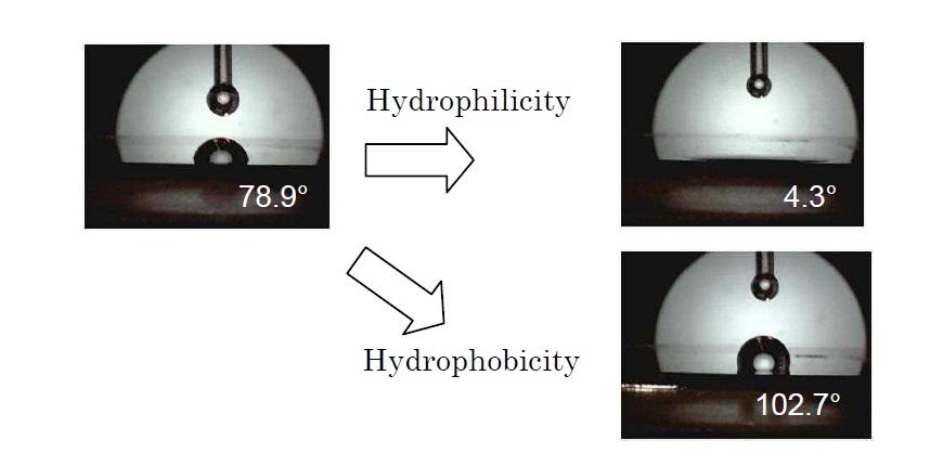
3. Surface treatment (Hydrophobicity from/to Hydrophilicity) - Pretreatment for wet process such as plating, etc., Pretreatment for underfill
4. Resin material ashing
5. Seed layer Ti etching
6. SiO2/SiN etching
Process performances
Descum*1

Etching uniformit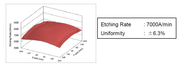 y: <± 10%(□500mm substrate)
Surface treatment (contact angle)
System appearance
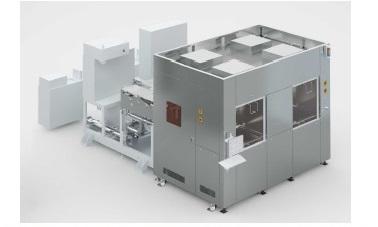
Dry etching system NA-1500
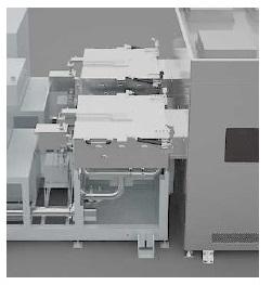
Process chamber
Future prospects
We consider that electronic components are required to be smaller and thinner, to provide higher-speed processing and to work on lower power with the developments in IoT, and manufacturing technologies of advanced packaging become more important.
ULVAC meets customer's future needs for flexible, invisible or wearable devices.
*1Descum : Removal of residue (scum) in photolithography of photopolymer
*2CCP : Capacitive Coupling Plasma
*3Desmear : Removal of residue (smear) in Via formation with laser drill
For further information
Advanced Electronics Equipment Sales Dept.
Corporate Sales & Marketing Division I
ULVAC, Inc. elec_info
TEL: 81-467-89-2139 / FAX:81-467-89-2297
Web site:http://www.ulvac.co.jp/en/
http://www.ulvac.co.jp/products_e/