This post is also available in: Japanese Chinese (Simplified)
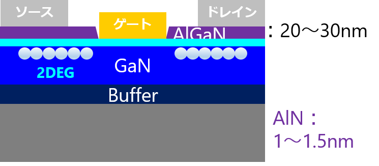
There are several gate structure patterns in GaN HEMTs, but all of them require very shallow machining.
Challenge
Keep good rate condition
Less damage as much as possible
Selective etching
Solution
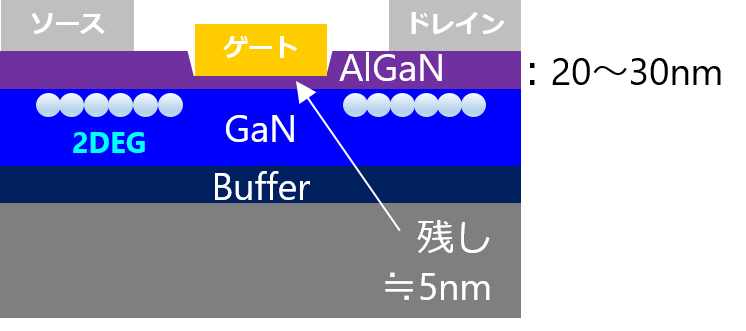
Forming recess structure
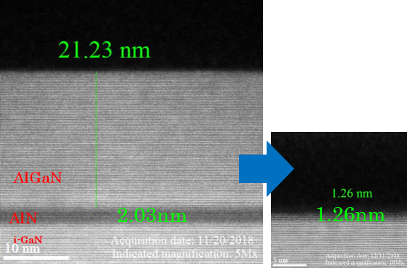
Very low rate etching leaves a small amount of AlGaN. (Example of leaving 5 nm by 25 nm etching)

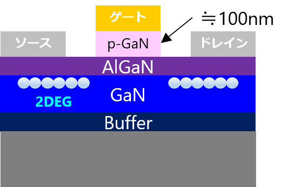
Forming P-type GaN layer
Etching p-GaN only, leaving AlGaN

Forming AlN spacer
Deposition 1 ~ 1.5nm AlN, etching AlGaN