This post is also available in: Japanese Chinese (Simplified)
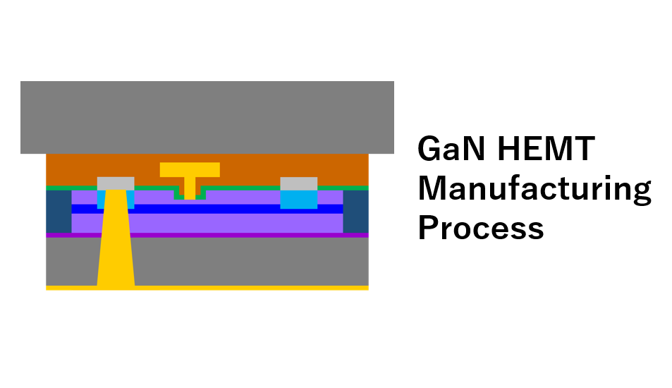
GaN HEMT (High Electron Mobility Transistor) is a next-generation power semiconductor that has low operating resistance and high breakdown withstand voltage, and is expected to be applied to high-power and high-speed electronic devices.
GAN HEMT Fabrication flow
 |
1. Forming GaN Epi layer |
 |
2. Ion implantation N+ |
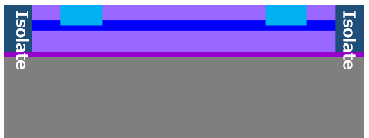 |
3. Isolate Ion implantation |
 |
4. AlGaN recess or selective etchingThe indented structure for forming the gate requires very shallow machining. Very low rates, selective etching, and no damage are important. |
 |
5. SiN gate isolation film |
 |
6. Pattering SiN gate isolation filmLow damage etching is required |
 |
7. Forming gate electrode & LiftoffLiftoff evaporation is used to form gate electrode. |
 |
8. Forming S/D electrode & PatterningSputtering Ti/Al and etching to form electrode |
 |
9. Attaching support substrate & Polishing |
 |
10. Etching backside Via SiCVia processing the back side Si / SiC to connect the electrodes |
 |
11. Seed Metal
|
 |
12. Plating |