This post is also available in: Japanese Chinese (Simplified)
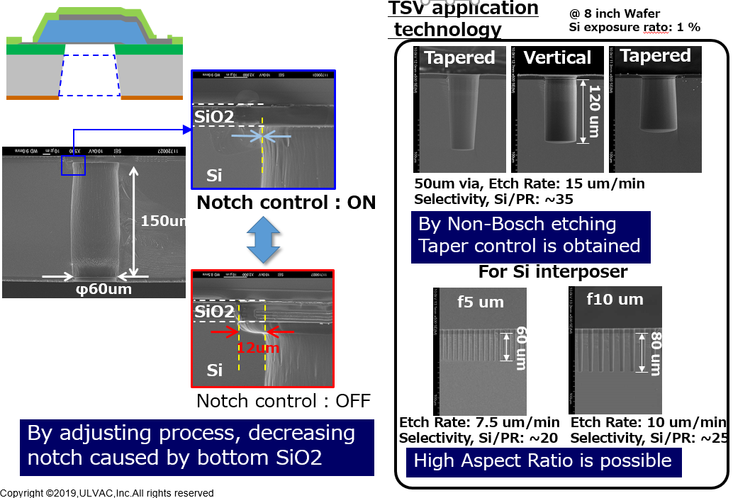
Backside Via etching
The possible causes of the notch are as follows.
(1) Due to the incident of cations on the bottom SiO2 surface
(2) SiO2 surface is just charged up
(3) Although the following incident cations enter the positively charged SiO2 surface
(4) Because the incident orbit is bent laterally due to the repulsive action on the positive charge on the SiO2 surface.
(5) A notch is formed by colliding with the side wall and etching reaction there.
To prevent this, “introduce a pulse power supply to alleviate the charge” on the lower electrode. In addition, we use TSV application technology to enable Taper control and high Aspect Ratio by Non-Bosch etching.
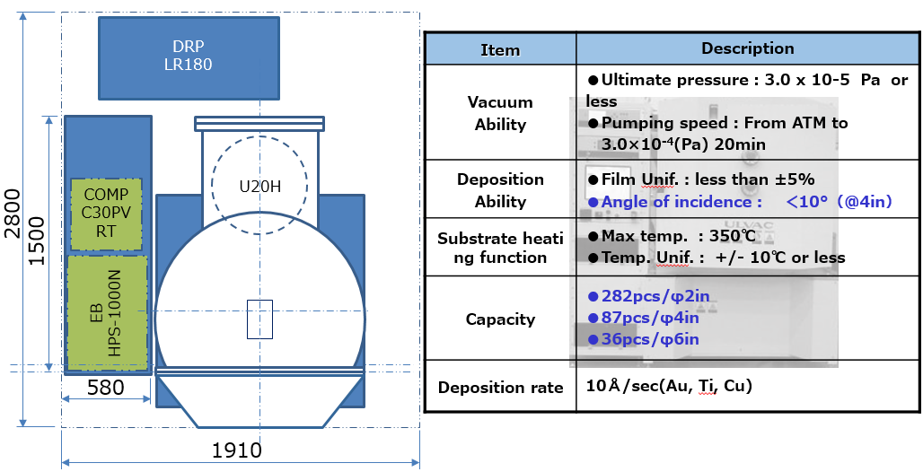
Contact electrode(Evaporation)
Liftoff and mass productivity
Contact Us
https://www.ulvac.co.jp/en/contact/elec_inquiry/
Baw Device fabrication flow
https://www.ulvac.co.jp/wiki/en/process_g_baw/
Pages: 1 2