This post is also available in: Japanese Chinese (Simplified)
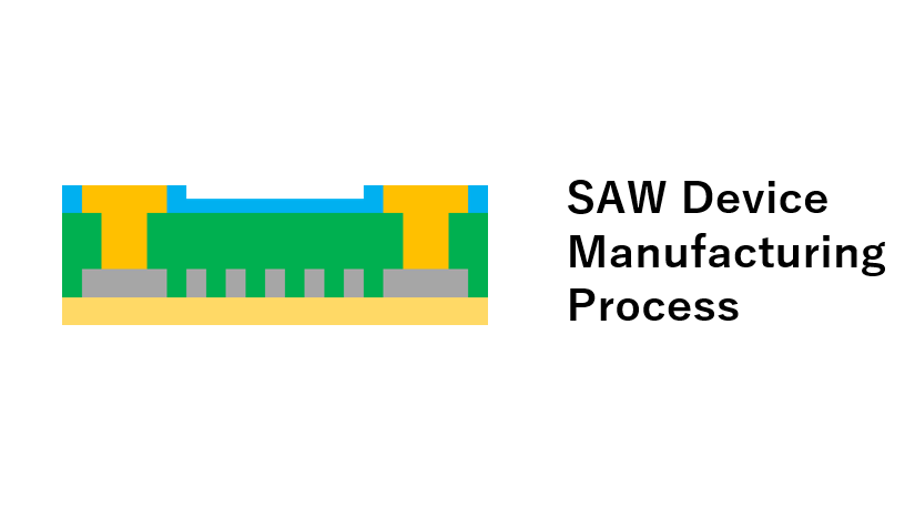
A SAW device is a filter device that has a structure that excites surface acoustic waves with a thin film of piezoelectric material or a regular comb-shaped electrode formed on a substrate.
SAW Device fabrication flow
|
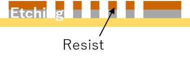
1A. IDT electrode process by sputtering and etching1A-1. IDT electrode depositionMetal (Al, Mo, W) sputtering, piezoelectric LT and LN are used for the substrate. The film thickness uniformity of this electrode is also important. Introduction of Sputtering system 1A-2. IDT electrode etchingSAW is an abbreviation for surface acoustic wave, and the frequency is determined by the Pitch of the IDT (comb tooth) electrode, so it is defined by Lithography and processing. The lift-off method has been used as a conventional technique for forming electrode patterns, but the dry etching method is required for fine processes where the distance between electrodes is 1 μm or less. (The relationship between frequency and IDT Pitch is approximately 1um width at 0.8GHz, 0.4um width at 2.5GHz, 0.18um width at 5.0GHz) Process technology for SAW device 1A-3. Removing ResistSupports residue removal after lift-off with ashing |
  |
1B. IDT electrode process with liftoff evaporation1B-1. IDT electrode evaporationThe film quality is Al, Cu. Achieves long-distance TS and improves film thickness uniformity. Process technology for SAW device 1B-2.Removing Resist Supports residue removal after lift-off with ashing |
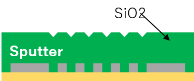 |
2. TC filmSiO2 deposition by sputtering |
 |
3. Adjusting film thicknessHalf etching of SiO2 |
 |
4. Making film smootherTrimming by ion milling |
 |
5. Contact hole |
 |
6. Contact electrodeMetal deposition by liftoff evaporation and removing resist |
 |
7. Forming encapsulation filmSiN sputtering |
 |
8. Adjusting film thicknessHalf etching of SiN |
 |
9. Making film smootherTrimming by ion milling |
 |
10. Making contact holeEtching SiN |
 |
11. Stripping resist and resdue |