This post is also available in: Japanese
As we progress into the future, the demand for high-performance devices in the areas of mobile, automotive, HPC, IoT, and server will most definitely continue to increase. Products in such industries require greatly diverse structures, depending on their desired function.
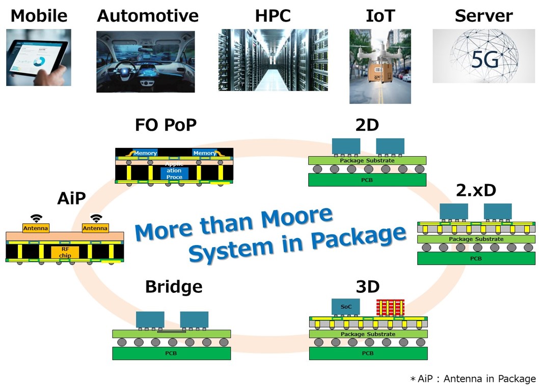
As the margin for further minituarization shrink, packaging technology continues to receive spotlight as a means to enhance device performance. Technology to integrate heterogeneous devices for higher performance is called More than Moore, and a device in which multiple semiconductor chips are sealed in a single package is called a System in Package.
Fan-Out package on Package is a structure that stacks memory on top of the application, used for mobile application processors.
Antenna in Package, as the name suggests, is a device that combines an antenna and an RF chip. It is effective in making the device smaller and faster in response time.
2D Implementation is a packaging in which multiple chips are connected by a package substrate.
2.xD (Dimension) Mounting is an application method where a high-density wire is inserted between the chip and the package substrate. It is a device structure used for high-end products such as high performance data centers. When an interposer is made of resin, it is called 2.1 D implementation, and when it is made of Silicon (Si) , it is called 2.5 D implementation.
Bridge is a mounting method in which chips are connected to each other by a finely patterned Si bridge. This method locally implements Si interposer.
3D implementation is a method in which chips are stacked together.
As such, the structure of a device varies greatly depending on the performance requirements of each device.
WLP (Wafer-Level Packaging) manufacturing process
Inquire here for ULVAC’s equipment for electronic appliance parts manufacturing