This post is also available in: Japanese
A build-up layer is the wiring layer of the substrate that utilizes build-up wiring.
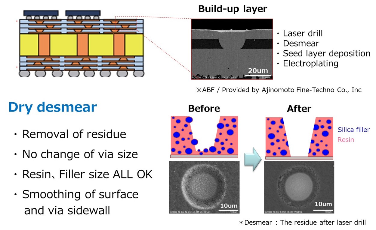
For wiring layers such as IC and PCB boards, it is common to use a compound material of glass filler and resin, such as Ajinomoto build-up film (ABF). Laser drilling is used to form via in these materials. The residue of the laser drilling is called “smear” and the process of removing “smear” is called “desmear.”
Performances required for a dry desmear process are:
- Removability of smear/residue
- Preventability of via enlargement
- Ability to work with unrestricted choice of resin type and silica filler size
- Ability to maintain surface smoothness
After a dry smear, if the surface roughness increases, the equipment’s high-frequency properties deteriorate.
In dry desmear, the process gas can be devised so that the etching rate of the silica filler and the resin line up, maintaining the smooth surface following the process.
This unique advantage of the dry process is a crucial technology for the future, as the wiring layer continues to become finer.
WLP (Wafer-Level Packaging) manufacturing process
Inquire here for ULVAC’s equipment for electronic appliance parts manufacturing