This post is also available in: Japanese
Fostering Future Researchers and Make Technological Progress for the Future through MEMS Development
Unlike the times of Edison, progress in science can no longer be achieved by a single scientist. In modern science, research projects are interdisciplinary, pressuring researchers to get results as early as possible. This is also true of development of MEMS (Micro Electro Mechanical Systems) which can be applied to an increasing number of fields. Dr. Yoshio Mita, Associate Prof. at the University of Tokyo is involved not only in research and development of MEMS, but also in development of next-generation researchers and management of industry-government-academia projects. In this issue’s Vision, we asked Dr. Mita about promising MEMS technology as well as teaching methods to ensure further progress in this technology as well as his views on the qualities and mindset required for researchers.
Associate Professor, Department of Electrical Engineering, School of Engineering, The University of Tokyo
Affiliated Professor to the VLSI Design and Education Center (VDEC)
Manager of the Microfabrication Platform Project in the Nanotechnology Platform Project
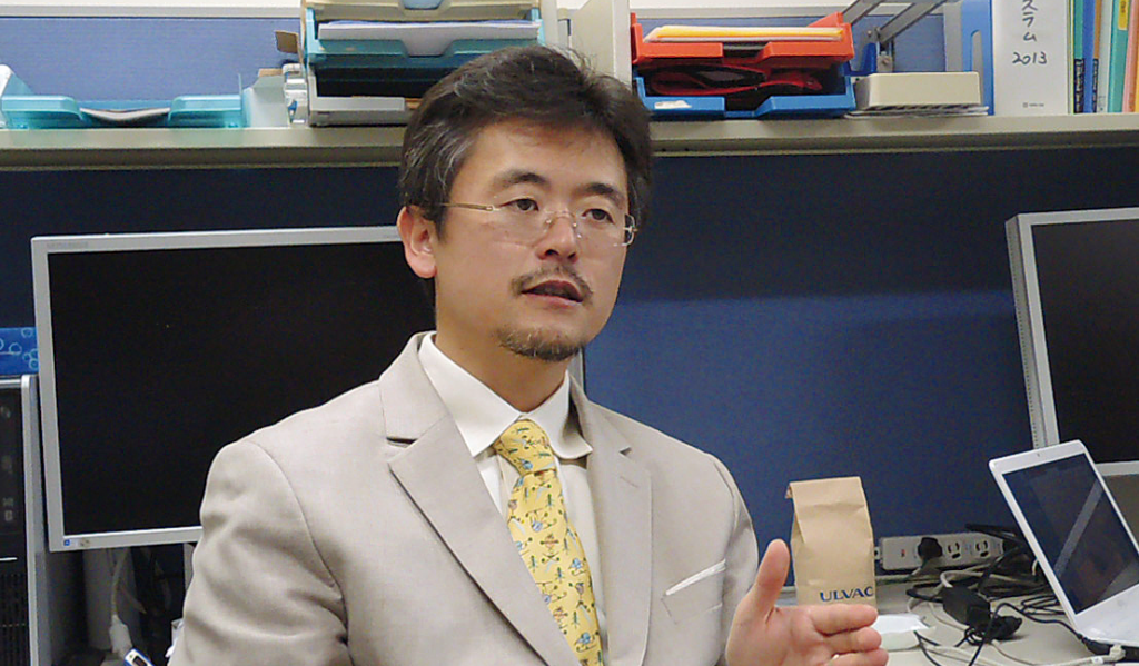
Dr. Yoshio Mita
*This article was released in “PR Magazine No.64 published in April, 2014”
Introduction: Origin and Technological Development of MEMS
MEMS (Micro Electro Mechanical Systems) generally refers to ultra-tiny machines on the micron scale (1/1,000 millimeters) and this field is also sometimes called “micro mechatronics” or “micromachines”.
The first person who mentioned the great potential of MEMS is Richard P. Feynman a prof. at California Institute of Technology and who also jointly received the Nobel Prize in Physics along with Shinichiro Tomonaga in 1965 for his contribution to progress in the field of quantum electrodynamics. In a lecture called “There’s plenty of room at the bottom” held at the university in 1959, he made ten proposals about the potential of the nanoscale world.
There is an interesting episode about Feynman. He announced he would offer a $1,000 prize to anyone who could make a micromotor with a diameter of 1/64th of an inch (approx. 4 millimeters). It was easily realized by an engineer in 1960 the year following the lecture, and to whom the prof. paid the prize money.
It is an undoubtable fact that this opens up new unexplored field of MEMS.
In the 1970s and 1980s, much technological progress was made in MEMS while widening its applicability to fields such as semiconductor pressure sensors and movable mirror arrays.
As motors similar to the micromotor for which Feynman offered prizes, Prof. Y. Tai from the University of California, developed a micromotor using metal and silicon thin films in 1989 while a Japanese research group led by Prof. Hiroyuki Fujita at the Institute of Industrial Science, The University of Tokyo, developed an electrostatic rotary motor in 1987 and an electrostatic nickel-plated micromotor in 1991.
These motors used semiconductor processes such as thin-film deposition, pattern formation (photolithography) and etching which have become mainstream technologies since then. Prof. Fujita is still active as a leading Japanese MEMS researcher who taught and greatly influenced Prof.
Deep Etching Technology Contributing to the Three-dimensional Structure of MEMS
Mita: Prof. Fujita is my respected teacher in MEMS.
After completing my graduation research into parameter extraction methods for MOSFET devices at the laboratory of Koichiro Hoh (grandson of Hidetaro Hoh, who is famous for the Hoh-Thevenin’s theorem), I researched smart micromachines containing integrated circuits (Smart MEMS) under Prof. Fujita’s guidance in my master’s and doctor’s programs. In this research, I proposed a sensor, processor, and actuator integrated system concept together with related fabrication technologies such as silicon shadow mask direct fine-patterring with self-alignment capability and micro
optical integration system.
MEMS technology is continuously making progress. Surface micromachining, which processes thin films into structures two-dimensionally was prevalent in the early days, but progress in silicon deep etching using ICP-RIE (Inductive Coupled Plasma-Reactive Ion Etching) and wafer bonding process technology has now made it possible to fabricate sophisticated, complex, three-dimensional structures.
This technological progress has contributed greatly to the progress of MEMS.
Microfabrication including deep etching is also one of my specialties.
When I started my postgraduate research in the new laboratory, I suffered from differences in the research environment.
At that time, I was feeling cocky just because my graduation thesis based merely on a little personal inspiration, was adopted for an oral presentation at an international conference. Since I have always liked electronic work, I was confident of being skillful with my hands. When I tried to make a micromachine myself, however, I lost confidence.
I couldn’t do as well as my seniors, even though we used the same devices and process. I kept thinking “why” everyday.
It was around the end of my second year in the doctoral course when I was finally able to to design a process just as I wanted and make a satisfactory micromachine according to the process without errors. It is due to this experience that I advise my students to be patient because it takes at least four years for them to do things just the way they really want (so they should not give up and should continue with their doctoral course studies).
Development of a Pond-Skater Robot Leading to Future Technological Progress in MEMS
MEMS technology is essential to the manufacturing of small high-performance electronic devices typified by sensors, printer heads, gyroscopes and projectors used in cars, optical devices, communications devices, and other manufacturing devices. MEMS which is now more integrated and composite, is used for developing multi-functional electronic devices. The future is thought likely to provide technology combining nanotechnology with biotechnology and the size of the MEMS market is estimated to grow from about 7.1 billion US dollars in 2010 to 11.3 billion US dollars by 2015.
Mita: I have been working to develop a pond-skater robot as one of my “toy (future dream)” projects. It may just be a “toy”, but it is a toy for the distant future. I believe that the more distant is the better.
When I studied at the University of Edinburgh in the U.K. in May 2007, I started researching towards a small, autonomous, self-propelled electronic device capable of running on water or to put it plainly, a pond-skater robot.
This kind of research drawing inspiration from living creatures was being conducted by many researchers in their own particular fields, but I thought a subcentimeter device capable of running on water under its own power would be the first of its kind in the world. In fact, there are other researchers researching similar robots around the world. I felt relieved and motivated by finding that these researchers also face technological challenges similar to mine.
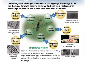
A permanent mission for researchers is exploring a field untrodden by others. It is my research style to focus on dreamlike applications. The world’s first novel approach involves various technological challenges. Overcoming these challenges requires making serious engineering efforts.
If we succeed in these efforts, we can obtain advanced technology which can be readily applied to diverse fields. I call this particular system a university-centered linear model for the 21st century (Figure 1).
Future Development of MEMS Requires Fostering Future Researchers
MEMS will be used in a wide range of industries. Research and development of MEMS involves more than just one academic discipline so universities can do more in the field of MEMS. Universities should also play a major role in fostering MEMS researchers.
Mita: While working as a researcher, I teach students at the UTokyo Hongo campus. If my left hand is for research, then my right hand is for education. I’m also responsible for the microfabrication project of the University of Tokyo in the Nanotechnology Platform Project led by the Ministry of Education. I feel like I manage the project with my “feet”. With my hand and feet always bound, I just want to keep my brain running free.
As an educator, I think it is important to give my students in the style that anyone can understand.I bring self-made teaching materials to my classes on electronic information devices and do experiments with these teaching materials in front of students.

As my students seem to like this style of teaching, I received the first “Best Teaching Award of the Faculty of Engineering, the University of Tokyo” this year.
I often encourage my laboratory students, saying: “You should first complete any project by yourself. It can be just a toy ploblem (future dream). By doing this you will learn a lot. If you face any problems, Don’t worry, I will help you.”
The largest difference between Japanese and French researchers I noticed when I was in France for study is that French researchers are without doubt
descendants of Descartes. They first doubt what others say. They don’t trust others in the first place. They build their logic based on only what they can trust.
I was surprised by their pragmatic approach. This approach is effective in fostering experts yet limits their interest in their own fields. This is a kind of division of work like a player’s position in rugby. On the other hand, Japanese researchers work like kendo players in a team competition.
It’s a team competition, but the players compete one by one. This is the Japanese style.
The philosophy of my laboratory consists of the best parts of the European style and the Japanese style. I want to develop “specialist” researchers who specialize in a certain field, as well as “ace” researchers, who are familiar with many fields. This is my ideal approach.
To accomplish this ideal, I try not to give answers to students straightaway. While I might tell high school students or younger students to do something according to a given method, I tell university students to do something according to a method that they came up with on their own. A method is an established approach with which anyone can produce the same results. It is more important for students to discover and master their
own method.
Persistence Will Pay Off. Every Failure is a Stepping Stone to Success.
Prof. Hiroyuki Fujita, a pioneer of MEMS in Japan, claims that three essential qualities of MEMS can be described with three M’s or namely Micro, Mass production and Multifunction.
With these three qualities in mind, we can say the MEMS industry will grow to produce MEMS devices on a size scale from 1 nanometer to 10 micrometers. In the world of nanometers, if we could manipulate atoms and molecules as if by gene manipulation, then we could also apply MEMS to the medical and bioscience sector and many other sectors.

Mita: Academic disciplines related to MEMS research will keep expanding. What a single researcher can do on their own is limited. The Takeda Sentanchi Building of the University of Tokyo puts up a slogan “one step by one thousand researchers.” This slogan means if each of 1,000 researchers takes just one step, then they take a total
of 1,000 steps altogether. At present, 500 researchers use the clean room, so we are just halfway to that goal.
To achieve this goal, I need to have a closer relationship with university and corporate researchers. I hope corporate researchers will come back to university to feel refreshed and inspired and then bring back what they learned and use it as the core of new business. University research facilities should be filled with researchers who make continuous technological progress.
The books shown on the right are French comics titled “Les Shadocks”, which are well known by all French. The main character is foolishly honest. He attempts an experiment which only has a one-ina-million chance of success for example by performing one million experiments.
He believes that even if he fails 999,999 times, he will succeed in his last attempt.
He is in fact ridiculed in the comics, but I believe this is where the truth of science lies—patience pays off. The more failures you experience, the more chances of success you have. You cannot succeed if you repeat failures aimlessly. Only if you reflect on your failures will you be able to find a new approach. This also applies to MEMS research. It is true that every failure is a stepping stone to success.
I’m working to achieve integrated MEMS through my research on pondskater robots. I want to share the findings of my research with others rather than keep them secret. To achieve “more than Moore” (progress of electronic devices through functional diversification), researchers from different fields should gather together to create new technologies by combining various technologies.
Dr. Yoshio Mita
Dr. Mita was born in Kure City, Hiroshima in 1972. After graduating from the Department of Electronic Engineering at the University of Tokyo in 1995, he completed his master’s course and the doctoral course (received a PhD in Engineering) respectively at the University of Tokyo in 1997 and 2000. From September 1997 to September 1998, he worked at the Institute of Electronics, Microelectronics and Nanotechnology (IEMN/ISEN) as an associate researcher at the National Centre for Scientific Research of France. His research achievement during his stint at the research institute was “A MEMS-Oriented Distributed Processor for Integrated Feed-Back Controller” which gained him the Yasujiro Niwa Outstanding Paper Award in February 2000. In April 2000, he became an assistant researcher at the VLSI Design and Education Center (VDEC) where he developed an efficient support system for open devices managed by the VDEC and achieved stable system operation. In April 2001, he became a lecturer at the Department of Electrical Engineering in the School of Engineering of the University of Tokyo, where he researched microsystems for integration with micro fabrication technologies,including intellectual VLSI, self-aligning peak fabrication technology, nano ridge fabrication technology, self-aligning rhombic micromirror fabrication technology, and microfabrication technology. Since April 2005, while serving as an associate prof. in the department, he has been conducting research in various fields ranging from nanofabrication technology and LSI integration technology to application systems at the Takeda Sentanchi Building.
*This article was released in “PR Magazine No.64 published in April, 2014”