This post is also available in: Japanese Chinese (Simplified)
1.Introduction
In recent years, OLED (Organic Light Emitting Diode) devices have started taking root even in the general consumer market, primarily in the displays of mobile phones and large-screen televisions as well as special/decorative lighting. Flexible displays and flexible lighting devices are expected to be a next-generation device employing the characteristics of OLEDs, and several companies are in the midst of a hot competition to develop devices, materials and equipment.
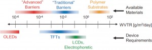
The development of OLED devices1) began nearly 3 decades ago, with extension of devices’ service life being one of the most important development items. Major decisive factors of a device’s life are moisture and oxygen2). OLED devices react very sensitively with such substances, which leads to the degradation of the element. For example, a comparison with other electronic devices (semiconductors (TFT), LCDs, etc.) in terms of water vapor transmission ratio (WVTR, g/m2/day) shows that OLED devices require encapsulation performance with the transmission ratio that is 100 to 100,000 times lower (high barrier property) (Figure 1)2). So far, glass and metal sheets have been adopted as the materials for encapsulating OLED devices3). For flexible devices as well, the use of ultra-thin glass has been attempted, however, it is not considered suitable as an ultimate encapsulation material for flexible devices as it is a “breakable” material3). Metal sheets are applied to bottom-emission type flexible devices in some cases3). In recent years, however, since it cannot be applied to a top-emission structure, which is a means of increasing the emission efficiency of OLED devices, opportunities to use metal sheets in flexible devices have decreased.
Given such circumstances, thin film encapsulation technology has attracted attention as an encapsulation technology for flexible devices. Our company began the development of encapsulation technology in 1999 and thin film encapsulation technology in 2010. We have since refined the process technology while improving the equipment based on the accumulation of device evaluations from domestic/overseas clients4). As a result, we completed the thin film encapsulation equipment, called the CEE-950, and delivered it to clients who then used it for the development and production of devices.
2.Thin film encapsulation technology
The current mainstream thin film encapsulation technology for OLED devices is to provide a laminated structure consisting of a barrier film, which protects OLED elements from moisture and oxygen in the atmosphere, and a buffer film, which allows deposition of the barrier film on the surface of the OLED elements with good cover-age5).
Candidate materials for barrier films include PECVD SiNx film6, 7), PVD AlOx film5) and ALD AlOx film8-10), and the development and evaluation of such materials are under way by several companies. PVD AlOx has a strong barrier property given its relatively thin film thickness (to 50 nm)8), and for this reason, it was widely used at the beginning of the development of thin film encapsulation technology. However, it started to become known that damage attributable to the plasma used in the PVD method was affecting the characteristics of the OLED devices9). and therefore, PVD AlOx film has gradually stopped being used. ALD AlOx allows the formation of a conformal film with high coverage and is considered a promising candidate as a barrier film10), though the sole application of ALD AlOx is not considered realistic due to its very low deposition speed, risk of film corrosion through direct contact with water11) and other reasons, and so its application as a barrier film in laminated layers with PECVD SiNx film or other films is also being studied.
Our company initiated the development of barrier films for OLED devices in 1999, and completed PECVD equipment for low temperature SiNx film deposition in 2001. At that time, low temperature SiNx was applied mainly as a temporary encapsulation (passivation) film based on glass encapsulation technology such as the Dam & Fill method.
One important characteristic of any barrier film deposition technique for OLED devices is the ability to perform the process at temperatures at which the OLED elements do not degrade. Low temperature SiNx film deposited by our low temperature (90℃ or below) PECVD equipment forms a superior barrier compared to other companies’ low temperature SiNx films, and satisfies the requirements as a barrier film for OLEDs including high optical transmissivity and low film stress. For this reason, many clients have adopted it. Our company’s thin film encapsulation technology employs this successful PECVD SiNx film as the barrier film for OLEDs.