This post is also available in: Japanese
3.Implantation characteristics
This section describes the stability and in-plane uniformity of the sheet resistance of phosphorus.
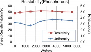
Phosphorus was implanted on the entire surface of one side of textured Cz wafers (156 mm, 0.5 to 6 [ohm・cm]) for N-type monocrystalline solar cells. Then the wafers were annealed (in a V8 furnace made by ULVAC) and the sheet resistance was checked. Fifty five hundred wafers were continuously implanted and the resistance was checked. The wafers were implanted with an implantation energy of 10 keV and a dose amount of 3.0×10¹⁵ [ions/
cm2].
Figure 5 shows the resistance and distribution of resistance values on the surfaces of the wafers. The average resistance is 50 [ohm/sq.] and the distribution between the wafers is ((Max-Min) / (Max+Min)×100)±4.0%.
The resistance is stable even in mass production. In addition, the wafer in-plane uniformity is less than 4.0%.
4.Patterning techniques
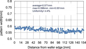
This section describes implantation using patterning masks. Boron was implanted on textured Cz wafers (156 mm, 0.5 to 3 [ohm・cm]) for N-type monocrystalline solar cells through masks. They were implanted with an implantation energy of 10 keV and a dose amount of 7×10¹⁵ [ions/cm2]. After the implantation, an optical microscope was used to check the widths of the implanted patterns.
Figure 6 shows the results of the implantation widths and locations. The average implantation width of masks is 570 μm and the distribution of the pattern width is ±4.0%.
The pattern widths can be controlled with this accuracy.
5.Conclusion
ULVAC has developed a compact ion implantation system for crystalline solar cells that can perform mask implantation.
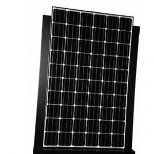
Wafers implanted with the system are highly stable. Figure 7 is an example of a solar cell module with cells that were mass produced with a“ PVI-3000N”.“ PVI-3000N” systems are already being used by customers in
the mass production of solar cells.
References
1) Andrew W. et al.: Appl. Phys. Lett. 55 (13) (1989), 1363.
2) J. Zhao, A. Wang, and M. A. Green: Prog. Photovolt. Res. Appl. 7 (1999), 471.
3) R. M. Swanson.: Proc. 33rd IEEE photovoltaic specialists Conference (2008).
Click here for Further information