This post is also available in: Japanese
1.Introduction
The solar battery market has been expanding around the world year after year because of the benefits of using solar energy as a renewable energy. There are various types of solar cells, a large portion of which are crystalline solar cells.Among mass-produced crystalline solar cells, conventional Al-BSF (back surface field) cells were mainstream, but in recent years mass production of high-efficiency cells, such as PERCs (passivated emitter and rear cells1), PERL (passivated emitter, rear locally diffused) cells2), and IBC (interdigitated back contact3) cells, became possible and their production is increasing. However, their manufacturing processes involve patterning and other complicated processes and thus the manufacturing costs are high. There is a need to simplify the manufacturing processes and reduce the costs.
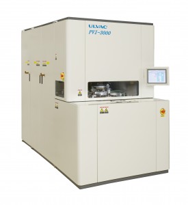
A solution to reducing the complexity of the manufacturing processes and costs is to use ion implantation using masks in place of the conventional complicated patterning techniques using lasers and etching. ULVAC holds a patent for an implantation technique using masks (patent number: 4252237). We developed the “PVI-3000” and “PVI-3000N” ion implantation systems for solar cells by drawing on our experience in the semiconductor sector.
These systems can achieve highly accurate patterning by mask implantation.
In this paper, we will introduce the features of the“ PVI-3000N” ion implantation system for crystalline solar cells and explain the characteristics of implantation and ion implantation patterning techniques using masks.
2.ULVAC“ PVI-3000N”
This section introduces the “PVI-3000N” ion implantation system for crystalline solar cells.
The“ PVI-3000N” has the features listed below.
a ) High throughput (1000 wafers per hour)
b ) Small footprint
c ) Capable of implanting ion species (phosphorus or boron)
d ) Mask implantation (Patterning and edge cut)
e ) High alignment accuracy (within±50 μm)
f ) High operation rate (at least 90%)
This system is unique in that it achieved high throughput with a small footprint while being capable of highly accurate patterning using masks.
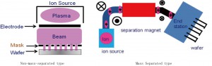
Figure 2 illustrates a schematic diagram of an ion source. The ion implantation system for crystalline solar
cells uses non-mass-separated ion implantation that canimplant at higher current than the mass separation type,
obtaining high throughput. Unlike mass-separated ion implantation systems that are mainly used for semiconductors, the non-mass separation type has no mechanism for separating ions, so it has the advantage of a smaller footprint.
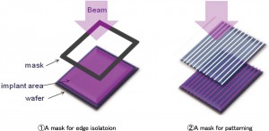
Figure 3 illustrates a schematic diagram of masks. The image on the left shows a mask for edge isolation and the image on the right shows a mask for patterning.
Implantation using the mask in the left image can isolate edges, which has the advantage of making it possible to omit the isolation process. This technique is useful for all solar cell manufacturing processes in which edge cutting is performed. A patterning mask like the stripe pattern mask shown in the right image in Figure 3 is used to form a pattern on a wafer. Up to three masks can be mounted in the system at once, enabling the edge isolation mask to be used in combination with the stripe pattern mask, for example, and the system can be used for up to three masking processes.
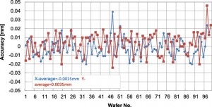
The system has an alignment mechanism to align masks to each wafer at an accuracy of ±50 μm. Figure 4 is a graph in which the distances between the positions after alignment and the mask centers are plotted for 100 wafers processed in a row. The graph shows that the differences are within ±50 μm after alignment for both the Xand Y-axis directions. As patterns of high-efficiency cells become finer, alignment needs to be more accurate, so
the “PVI-3000N”’s mechanism for aligning each mask to each wafer is essential to successful patterning.
Click here for Further information