This post is also available in: Japanese
1.SiC power device introduction
Power electronics play an essential role in the construction of smart cities and as part of the solution to global warming. Power electronics are used to convert and control electric power in various applications, such as electric trains, automobiles, solar cells, and air conditioners. Power devices, the key component of power electronics, are required to deliver high performance, such as low power loss and high switching speed.
Figure 1 illustrates the relationship between various power device applications and semiconductor materials used to manufacture the power devices in the power electronics market. The horizontal axis denotes operating frequency, and the vertical axis denotes switching power. For the last several decades, Si has been mainly used as a semiconductor material for power device production.
However, power devices based on Si are approaching their theoretical performance limits determined by the physical properties of Si. Expectations for a major breakthrough in power electronics using Si-based power devices are all but gone. As a substitute for Si, wide-band-gap semiconductors (SiC, GaN, and diamond) are promisingmaterials. In particular, SiC has found wider application in various areas than other materials, and the development of SiC-based devices has been advancing. Compared with Si, SiC has about three times the band gap, about ten times the dielectric breakdown field, and a higher BFOM (Baliga’s Figure of Merit) by two orders of magnitude.
BFOM is an index indicating the performance of power devices, and this higher BFOM suggests that operating resistance, an essential factor in achieving low power loss, can be reduced by a factor of 2001 1)-3).
In order to launch SiC devices into the market, our Advanced Electronics Equipment Division has developed an ion implantation system and an activation annealing system for SiC production, and our Institute of Semiconductor & Electronics Technologies has developed a SiC process and mass production technologies. In addition, we teamed up with TPEC (Tsukuba Power-Electronics Constellations) to develop a mass production process for SiC devices, to conduct verification tests on SiC devices, and
to refine the equipment.
TPEC was inaugurated in April 2012, as a base organization for promoting the development and spread of mass production technologies for SiC power semiconductors in industry-government-academia collaboration. From 2010 to 2012, the National Institute of Advanced Industrial Science and Technology, Fuji Electric Co., Ltd., and ULVAC, Inc. cooperatively conducted an Industry Innovative Research Initiative entitled,“ Research on Trial Production for SiC Device Mass Production and Verification of System Application.” TPEC inherited this activity and has been continuing the research.
This article mainly describes the results of tests performed in the process of developing mass production
technologies for SiC devices, reporting the process of ion implantation and activation annealing and the results of characteristic evaluation of modules constructed by combining prototype devices, SBDs (Schottky-Barrier Diodes) and MOSFETs (Metal Oxide Semiconductor Field-Effect Transistors).

2.Overview
2.1 Key technology for SiC process
While the SiC device process has a major advantage in that technologies for the Si process can be used for it, one reason SiC devices are harder to produce than Si devices is that the diffusion coefficient of SiC materials is so small.
Due to their small diffusion coefficient, the thermal diffusion technology used for the Si process is not applicable to the SiC device process. Accordingly, we use ion implantation technology instead of thermal diffusion technology and implant ions at several levels of energy to form a box profile. In the Si process, room-temperature implantation is generally used. On the other hand, in the SiC device process, implantation needs to be performed with the SiC substrate maintained at a high temperature in order to suppress 3C-SiC growth during the activation annealing
process after implantation. Otherwise, 3C-SiC will reduce the channel mobility of the SiC devices.
In the conventional Si process, activation can be achieved at approximately 1,000℃, whereas in the SiC
process, high-temperature annealing at 1,600℃ or higher is required due to the strength of the bond of SiC molecules.
In addition, in a high-temperature process, the evaporation of Si atoms from SiC molecules causes rough
surfaces, leading to a reduction in channel mobility. To prevent this phenomenon from occurring, the carbon cap process is needed to suppress the evaporation of Si atoms.
The activation annealing technology needs to satisfy these requirements. Unlike oxide-layer (SiO2) formation from a Si layer in the Si process, in the gate oxide process of the SiC process, an oxide layer is formed from a SiC layer. Consequently, C atoms remain in the interface which raises the interface state
density. To eliminate this problem, studies on various methods for decreasing the interface state density have been actively carried out. 4H-SiC, which is used for device production, has two C-planes, a silicon face (0001) and a carbon face (000-1). The silicon face and carbon face of 4H-SiC have different dangling bonds and therefore their surfaces and interfaces exhibit different physical properties. For example, thermal oxidation of the carbon face progresses several times faster than that of the silicon face. Accordingly, conditions for forming a gate oxide layer need to be optimized separately for each crystal face. Generally, dry oxidation using oxygen and nitridation using nitrogen monoxide are used for the treatment of the silicon face, and wet oxidation and H2 annealing (mentioned later) are used for treatment of the carbon face.
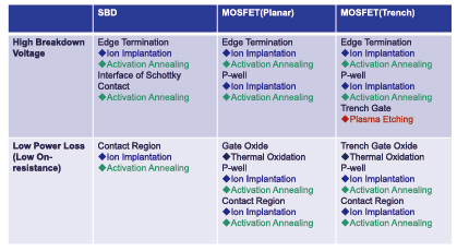
Table 1 lists the above-mentioned key process technologies used for the production of SiC power devices (SBDs, planar MOSFETs, and trench MOSFETs). Device performance is determined more by production processes than by device combinations and physical properties. Accordingly, Table 1 shows device regions and the important processes that are applied to the device regions to determine device performance related to dielectric strength and power loss (particularly on-resistance).
The ion implantation and activation annealing technologies are key process technologies common to all SBDs, planar MOSFETs, and trench MOSFETs.
The above-mentioned key process technologies are used for various device regions requiring higher dielectric- strength performance, for example, the device edge regions and Schottky contact interfaces of SBDs and the device edge regions and P-well regions of planar/trench MOSFETs. In the process of fabricating trench MOSFETs, in addition to these process technologies, plasma etching technology is also used to form trench gate regions.
The above-mentioned key processes are also used for various portions requiring higher performance related to power loss, for example, the contact regions of SBDs and the contact regions, P-well regions, gate oxide layers, and SiC interfaces of planar/trench MOSFETs.
2.2 Process system
This article introduces some mass-production models that are particularly important for SiC device production. These models have been created from the base systems used at TPEC.
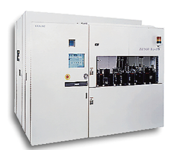
The IH-860DSIC mass-production ion implantation system (Figure 2) provides the following features.
a) High throughput
b) High-temperature implantation using an electrostatic chuck (up to 500℃)
c) Dual end station switchable between room-temperature implantation and high-temperature implantation
d) Multiple energy ion implantation for forming box profiles (maximum energy: 860 keV, operation using double charged ions)
We conducted implantation under conditions for a box profile (30–300 keV; 5×1018 cm-3) followed by activation annealing at 1,600-2,000 ℃ . Subsequently, we conducted measurement by SIMS (Secondary Ion Mass Spectrometry) and verified that the IH-860DSIC performs both highenergy and high-accuracy implantation (in terms of energy and dose amount) as shown in its simulation. We also observed that the dopant profile does not vary with the annealing temperature (1,600-2,000℃). This suggests that the dopant does not drive in by thermal diffusion.
2.3 Results of tests using key processes4)
(1)Ion implantation
As mentioned in Section 2.1, high-temperature implantation is essential for removing accumulated implantation damage. We implanted Al into SiC substrates by roomtemperature (RT) implantation and high-temperature (500℃) implantation followed by high-temperature annealing and measured the RHEED (Reflection High Energy Electron Diffraction) pattern to evaluate the effect of the high-temperature annealing. The implantation conditions were 30-300 keV and 5×1018 cm-3. In this evaluation, we compared SiC substrates that underwent the following four implantation patterns: RT implantation alone, RT implantation followed by 1,700℃ annealing, 500℃ implantation alone, and 500℃ implantation followed by 1,700℃ annealing. According to the results of the RHEED measurement, no damage accumulated at an implantation
amount of 5×1018 cm-3. We also measured the electrical characteristics and found that the mobility and the sheet carrier concentration were almost same between RT implantation and 500℃ implantation.
We conducted a similar test under a high dose condition (2×1020 cm-3). The RHEED patterns obtained were completely different from those obtained for an implantation amount of 5×1018 cm-3. A distinct halo-like pattern was observed after implantation, and 3C-SiC was detected on top of 4H-SiC after RT implantation followed by 1,700℃ annealing. This fact suggests that an amorphous layer was formed after the RT implantation, and that 3C-SiC developed during the 1,700℃ annealing. We measured the
electrical characteristics and found that the electrical characteristics also exhibited a similar difference as seen in the results of the RHEED patterns.
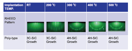
We measured the RHEED patterns (Figure 4) to evaluate the effects of Al implantation temperature and hightemperature annealing.
It has been found that 3C-SiC is growing below 200℃, while 4H-SiC is growing above 300℃ after annealing.
(2)Carbon cap and activation annealing
We compared the effects of capless annealing, annealing with resist carbon-cap, and annealing with carbon-cap by sputtering. Capless annealing increased the surface roughness (Ra) significantly, Ra increasing to 13.3 nm by annealing at 1,900℃. In contrast, resist carbon-cap reduced Ra to 0.78 nm when annealed under the same conditions, and carbon-cap by sputtering further reduced Ra to 0.16 nm. AFM obser vation also showed that step bunching occurred on the surface during capless annealing.
We confirmed by AFM observation that carbon-cap by sputtering formed a flat and smooth surface during annealing (Figure 5). These results suggest that carbon-cap by sputtering delivers excellent performance in annealing at temperatures up to 1,900℃.
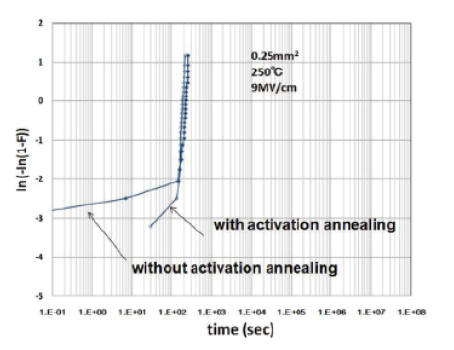
We made full use of high-temperature implantation, carbon- cap, and activation annealing to form gate oxide layers with a flat and smooth surface and verified the reliability of the gate oxide layers. In this process, the gate oxide layers were formed by wet oxidation, and MOS capacitors were fabricated from the formed gate oxide layers by H2 annealing. In the TDDB (Time Dependent Dielectric Breakdown) test on gate oxide layers formed on SiC surfaces annealed at 1,600℃ and gate oxide layers formed on without annealed SiC surfaces, an electric field of 9 MV/ cm was applied to the gate oxide layers at 250℃.
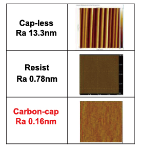
Figure 6 shows the Weibull plots of the lifetimes of the MOS capacitors. They indicate that there are no distinct differences between activation-annealed SiC surfaces and without annealed SiC surfaces. Therefore, the process consisting of ion implantation and carbon-cap annealing will not induce surface roughness and defects that degrade dielectric strength. We have concluded from these results that hightemperature implantation and annealing with carbon-cap by sputtering are suitable for mass- roduction lines.
2.4 IEMOSFET/SBD device fabrication5) at TPEC
we describe part of the performance of IEMOSFET (Implantation Epitaxial MOSFET)/SBD devices, which were fabricated at TPEC in cooperation with ULVAC and other organizations, and IEMOS/SBD modules.
At TPEC, we successfully fabricated an IEMOSFET device (with an on-resistance of 5.0 mΩcm2 and a dielectric strength of 1,200 V) and an SBD device (high avalanche withstandig capability and small Vf).
We compared the switching characteristics of a 1,200VIEMOSFET module and the latest IGBT module. The modules contained a packaged 2.5 mm×2.5 mm IEMOSFET and SiC-SBD. The IGBT was a combination of the latest 1,200-V Si-IGBT and a Si-FWD (Free Wheel Diode).
We evaluated their switching device performance by measuring their dependence on gate resistance (RG) under the turn-off characteristics of an applied voltage of 600 V and a drain current of 15 A (at 125℃).
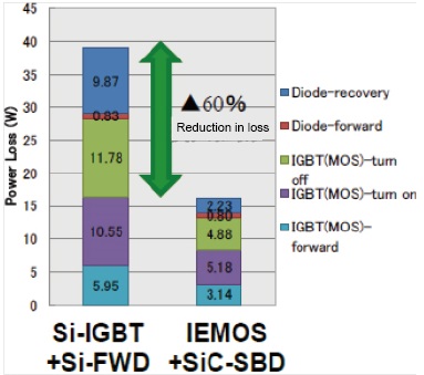
We compared switching losses, which depend on gate resistance (RG) at turn-off (at 125℃). The switching loss of the IEMOSFET was reduced by as much as 75% when no RG was connected, and was reduced by 57% even when RG was 68Ω. This fact suggests that the switching loss of the IEMOSFET module will be reduced in actual operation. For 20 kHz at 125℃, the power loss was reduced
by as much as 60% (Figure 7): 39 W for the IGBT module and 16 W for the IEMOSFET module. The current density of the IEMOSFET was 440 A/cm2, which is three times as much as that of the IGBT. Accordingly, it is expected that if its current density is reduced to be as low as that of the IGBT, the power loss of the IEMOSFET will be further reduced.
Thus, we have demonstrated with an actual prototype that the high-temperature implantation, multiple energy ion implantation, carbon-cap technology, and ultrahightemperature annealing technology that have been developed by ULVAC are suitable for mass-production lines for SiC-SBDs and MOSFETs. Further improvement of IEMOSFETs is progressing at present.
References
1) Kazuo Arai and Sadafumi Yoshida, Basics and Applications of SiC Devices, Ohmsha Ltd. (2003)
2) Hiroyuki Matsunami, Technology of Semiconductor SiC and Its Applications, Nikkan Kogyo Shimbun, Ltd. (2003)
3) NIKKEI ELECATRONICS 2013.4 90-95
4) K. Tezuka et. al., Mater. Sci. Forum 717-720, 821-824 (2012)
5) S. Harada et. al., Mater. Sci. Forum 717-720, 1053-1058(2012)
Click here for product information
IH860DSIC