This post is also available in: Japanese Chinese (Simplified)
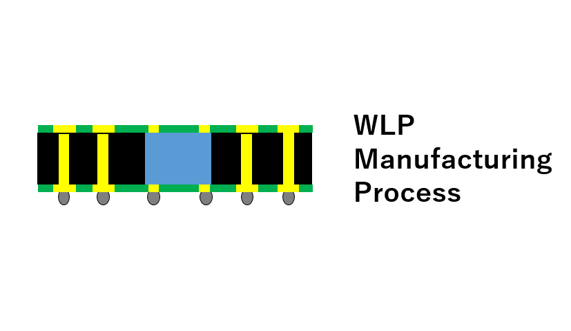
WLP is an abbreviation for Wafer-level Packaging, which is one of the mounting technologies expected as mobile devices such as smartphones become more sophisticated and thinner. ULVAC provides techniques such as sputtering, etching and ashing for the WLP manufacturing process.
Wafer-level Packaging (WLP) manufacturing flow
 |
1. Redistribution Layer(RDL)First layer |
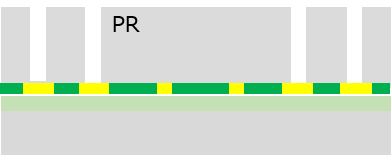 |
2. Photolitho ViaPerform Descum to improve the contact characteristics between Cu in the Seed layer and Cu plated. |
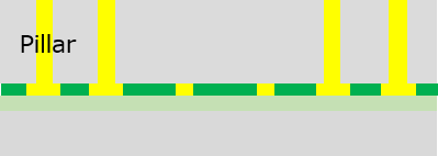 |
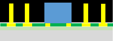
3. Cu PillarPlating Cu |
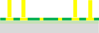 |
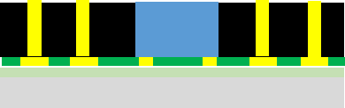
4. Removing Photolitho |
 |
5. Bonding Chip |
 |
6. Molding |
 |
7. Surface polishing |
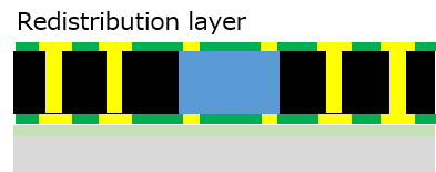 |
8. Redistribution layer(RDL) |
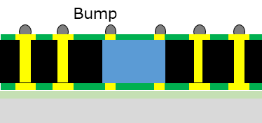 |
9. Forming Bump soldering |
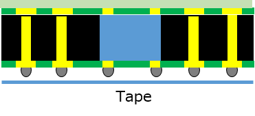 |
10. Placing one tape with dicing frame |
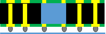 |
11. Removing strip layer |
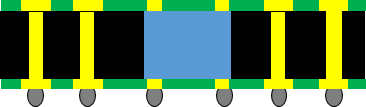 |
12. After dicing chips, stripping from dicing frame |