This post is also available in: Japanese Chinese (Simplified)
Introducing the dry etching technology required for the VCSEL process.
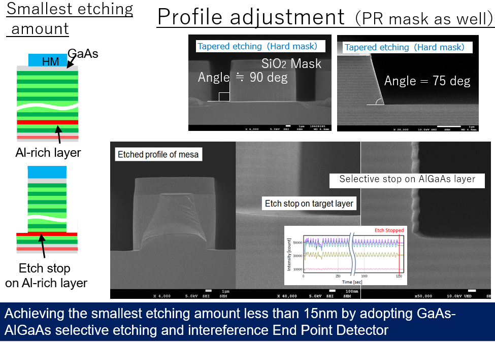
VCSEL Mesa process
Chlorine-based gas is used for etching group III-V compound semiconductors such as GaAs used in VCSELs. Since reactive-based conditions are used for AlGaAs / GaAs multilayer films, it is difficult to control the shape and in-wafer uniformity. Furthermore, in etching compound semiconductors, it is difficult to achieve both shape and in-wafer uniformity control based on process conditions alone.
Therefore, the NE dry etching equipment uses the ISM (Inductively Super Magnetron) method for the antenna structure. Antennas using the ISM method can optimize the plasma distribution, and a very uniform distribution of 3% or less can be obtained with GaAs wafers. The shape distribution based on the actual epi structure is also uniform.
For mesa depth control, the etching depth can be controlled with high accuracy by using the IEP (Interferometry End Point) system. The state of etching can be grasped from the interference waveform obtained by using this system. By counting the number of DBR pairs while monitoring this waveform, etching can be stopped at any depth.