This post is also available in: Japanese Chinese (Simplified)
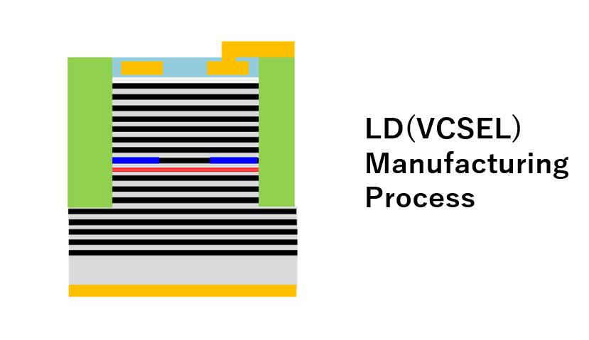
The market for semiconductor lasers is becoming active as a light source for 3D sensing technologies such as LiDAR, which are required for autonomous driving. As one of them, we will introduce a dry process for VCSELs (Vertical Cavity Surface Emitting Laser), which has merits such as miniaturization and energy saving.
VCSEL fabrication flow
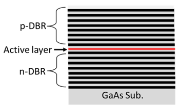 |
1. Epi growthOn a GaAs (gallium arsenide) substrate, AlGaAs / GaAs layers are epigrown as a laminated structure including a DBR (Distributed Bragg Reflector) multilayer film consisting of several tens of pairs or more and an active layer. |
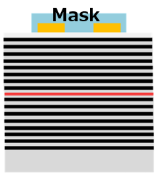 |
2. Patterning & Mask formingForm a mask pattern to form the epi layer into a column called a mesa |
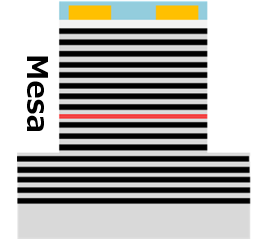 |
3. Patterning MesaPatterning Mesa by dry etching |
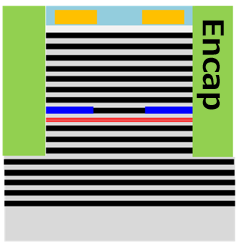 |
4. Forming active layer & encapsulationA specific AlGaAs layer designed near the active layer is oxidatively narrowed by wet oxidation (this oxidative narrowing layer is a very important layer that influences the characteristics of the VCSEL as a current and light confinement structure). It also forms a protective film on the side wall of the mesa. |
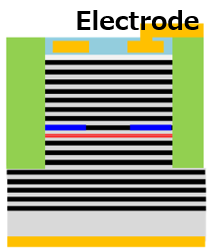 |
5. Forming electrodeElectrodes are formed on each of the n-type and p-type layers. |