This post is also available in: Japanese Chinese (Simplified)
Introducing the sputtering and etching technologies required for the MicroLED process.
Transparent conductive layer deposition
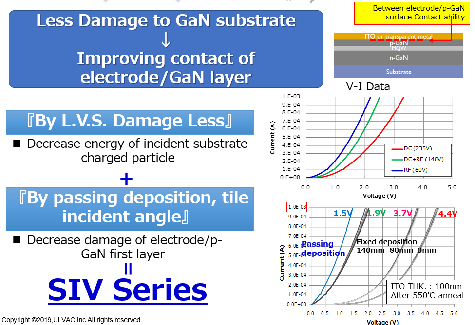
When forming an ITO film by the sputtering method, negative ions accelerated by an electric field near the TG surface enter the substrate at high speed and damage the ITO film on the substrate. LVS is a method of forming an ITO film softly with low damage by lowering the sputtering voltage (accelerated electric field of negative ions).
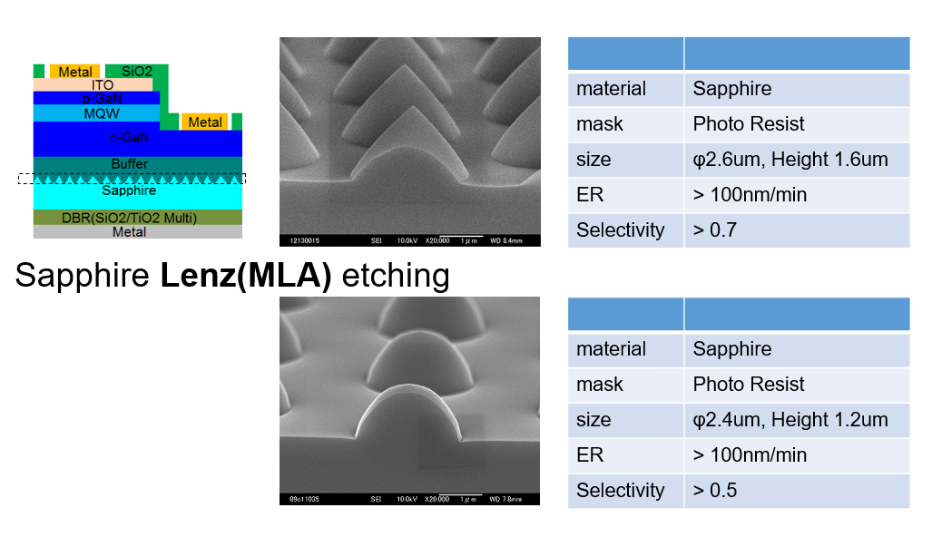
PSS process
Etching the surface of the substrate to create a conical shape and increase the light reflection efficiency.
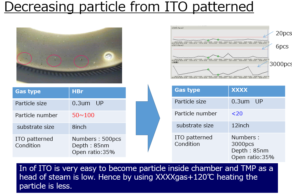
Etching for ITO process
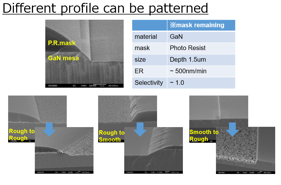
Etching (GaN Mesa)