This post is also available in: Japanese Chinese (Simplified)
The world’s highest level PZT sputtered film can be stably formed. (Coating on CMOS: PZT film forming temperature <500 ℃)
Equipped with a multi-chamber, PZT full stack (upper and lower electrodes + PZT) can be formed consistently.
Challenge
Low temperature process below 500 ℃
A low-temperature process of 500 ° C or less is required to mount piezoelectric MEMS on CMOS, but 600 ° C is required by sputtering for crystallization of PZT.
Both high piezoelectric performance and reliability
High throughput and high reproducibility for mass production
Solution
Use of buffer layer
Utilizes buffer layer to achieve PZT crystallization below 500 ° C
Hardware for PZT sputtering
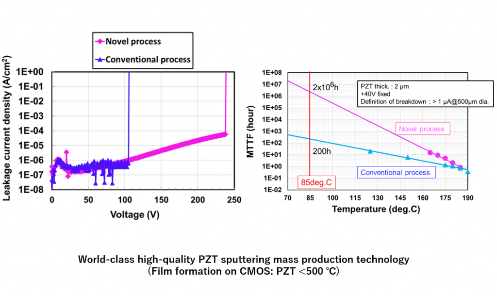
Excellent piezoelectric performance and high reliability in a low-temperature process of 500 ° C or less
Realize PZT configuration in the same device
Each stacked structure is formed in the same equipment for cluster type sputtering equipment
Specification of ULVAC PZT supttering
| Item | Specification | Advantage |
| Deposition temperature | <500 deg.C | On CMOS |
| Wafer size | 8 inch | Mass Production |
| Deposition rate | 4 μm/h | |
| Thickness uniformity | ±3.0% | |
| Pb content uniformity | ±0.6% | |
| Stress uniformity | Δ64MPa (Max-Min) | |
| Crystalline orientation | c-axis | High Performance |
| Morphorogy | Ra : 3.2 nm | |
| Piezoelectric coefficient :|e31| | ~ 15.5 C/m2 | |
| Breakdown voltage | ~ 200V (@2.0μm) | |
| TDDB(45V, 80 deg.C) | >2x 10⁶ hours | |
|
||