This post is also available in: Japanese
1.Introduction
In recent years, because of the rapid spread of mobile terminals typified by smartphones and tablets, IC chips are becoming increasingly thinner and smaler. Accordingly, there is a growing need for denser and thinner IC package substrates and the core layer, which supports a substrate, is becoming thinner and thinner1). On the other hand, larger chips, and accordingly larger substrates, are required for high-end servers, etc. To keep up with the trends and meet the needs for higher-density packaging in a wide range of fields from mobile applications to server applications, the use of semiconductor miniaturization technology for build-up wiring formation for PCB (Printed Circuit Board) substrates has been studied. PCB substrates are square substrate (panels) with a side length of 510 mm or more, and in addition to understanding warp- age, heat resistance, and their mechanical characteristics, there are unique challenges to tackle in handling various panels, challenges that are diferent from those in conventional silicon wafer processes2). This paper introduces the latest on ULVAC’s panel-level package solution, a technology released for the first time in the world.
*This article was released in “Technical Journal No.80 published in May, 2016”
2.Dry panel-level build-up process
2.1 Application of dry desmear with plasma etching technology
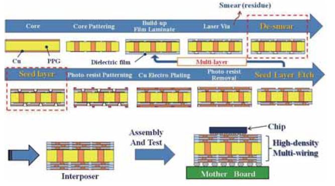
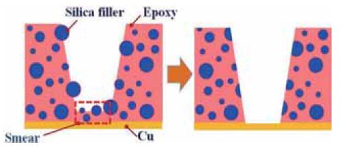
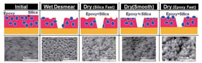
Figure 1 shows the PCB interposer production (build-up) process. A CO2 laser drill is used to form a via connecting the upper and lower insulating film layers. After via formation, residue called “smear” remains at the bottom of the via. The build-up film is made of a mixture consisting of epoxy resin and SiO2 particles called “silica filler” and this mixture is generally called a “glass epoxy film.” Smear consists of epoxy resin and silica filler as well. Proceeding to the next process without removing smear results in low wiring reliability, such as low adhesion of Cu and increased wiring resistance. Therefore, the desmear process is essential. With the current generation, smear can be removed in a wet environment, but various new challenges are arising because vias are becoming smaller and smaller (50μm or less). These challenges include, for example: (1) difficulty in applying the same wet processing conditions to different film qualities or adjusting these conditions; (2) limitations on controlling the dimensional conversion accuracy of micro vias (swelling problem); (3) limitations on the smoothness control of viasidewals; and (4) weakness of corresponding to high as- pect ratios (>2). Figure 2 demonstrates the need to shift from wet desmear to dry desmear3). As can be seen in the figure, with dry etching, smear can be removed and atthe same time, the irregularities on the silica filer on the via sidewal can be smoothed out. For this paper, A CCP-RIE (Capacitive Coupling Plasma-Reactive Ion Etch) etching system was used and ABF (Ajinomoto Build-up Film) was mainly used as the glass epoxy film.
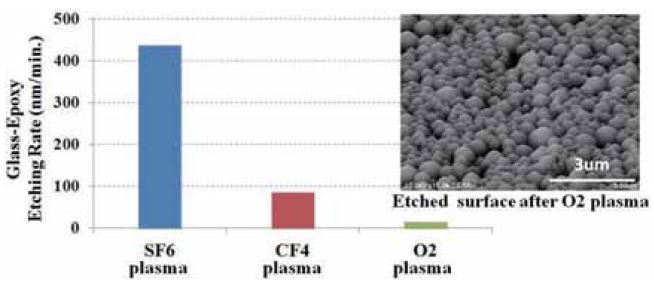
Figure 3 shows the etching rates ofthe glass epoxy films whose surfaces were etched with SF6, CF4, and O2 gases. The etching rate is highest when SF6 is used and lowest when O2 is used. This is because the silica filer cannot be etched with O2 only. Figure 4 shows the trends in the roughness of the glass epoxy surfaces etched with diferent mixing rates ofthese gases. From this figure, it can be seen that the smoothness of the etched surface can be controled by using the gas mixing rate that pro- vides nearly the same etching rate for the epoxy resin and silica filer. The surface with wet desmear is provided for comparison, comparison, which clearly shows that the surface with wet processing is rougher. These results can be consid- ered to demonstrate one advantage ofplasma etching, namely, that it is more suited to optimizing (adjusting) in- dividual plasma conditions (gas mixing rate and other pa- rameters) for each material and type than the wet process.
You can download full article with your registration
https://www.ulvac.co.jp/r_d/technical_journal/user_registration/
1) Y. Nakamura, S. Katogi; “TechnologyTrends and Future History of Semiconductor Packaging Substrate Material” Hitachi Chemical Technical Report (2013) No.55, 25.
2) A.Iwasawa, S. Sato, T. Nakamura, F. Echigo”Development of substrate for semiconductor packages using an insulator of low thermal expansion” 20th Micro Electronics Symposium,Ritsumeikan University, (2010)235.
3) Yasuhiro Morikawa, Muneyuki Sato, Yosuke Sakao,Tetsushi Fujinaga, Noriaki Tani, Kazuya Saito;“Fabrication of Ultra-Fine Vias in Low CTE