This post is also available in: Japanese Chinese (Simplified)
ULVAC provides technologies such as ion implanters and sputtering equipment for the manufacturing process of power device IGBTs. Power device IGBT (Insulated Gate Bipolar Transistor) is an acronym for Insulated Gate Bipolar Transistor.
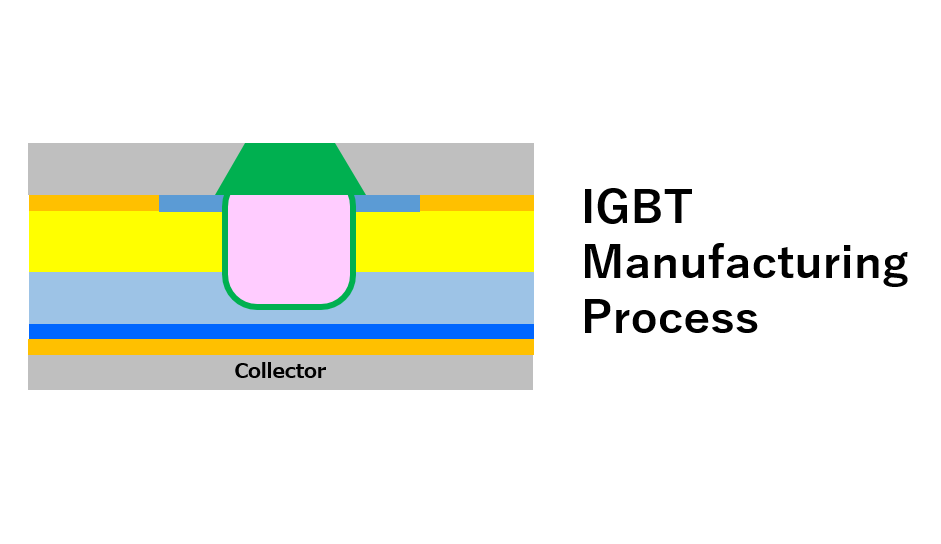
Power Device IGBT Process flow
 |
1. Substrate |
 |
2. B+ Ion implantationUsing Ion implantation equipment |
 |
3. Mask insulated layer formedUsing CVD |
 |
4. Mask insulated layer patternedPatterning insulated layer with etching and ashing |
 |
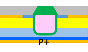
5. P+ ion implantationUsing Ion implantation equipment |
 |
6.Trench formedUsing etching equipment |
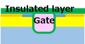 |
7. Insulated layer formed
|
 |
8. Insulated layer patternedPatterning insulated layer with etching and ashing |
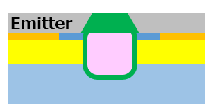 |
9. Emitter electrode formedUsing sputtering or evaporation |
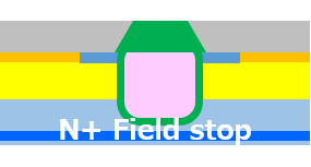 |
10. P+ FS layer formedUsing Ion implantation equipment |
 |
11. B+(Collector) formedUsing Ion implantation equipment |
 |
12. Collector formed
|
ULVAC Keytechnology
Ion Plantation
・ Improved IGBT performance by injecting phosphorus for the FS layer
・ Cost reduction by hydrogen injection for FS layer
Sputtering
・ Thin wafer transfer is possible
・ Stress adjustment
Etching
・ Supports Trench structure
PE-CVD
・ Low Damage Plasma driven at 27MHz
・ Stress control by substrate Bias is also possible