As expanding the market of microfluidics / microstructure devices in the biotechnology or life science fields, the demand for development of high volume manufacturing technique has been increasing. As one of the solutions, we have been developing a process to fabricate these devices on larger-format glass substrates.
In our previous study [1] [2], we reported wet etched glass mold for solder bumping technology which is called “C4NP”. The glass mold requires very precisely controllable etching technique. We achieved high accuracy and good uniformity pattern with wet etching in 300 mm whole wafer.
In this study, we applied this etching technique to biotechnology or life science applications. In addition, we combined wet etching, micro-blast for through-hole and direct bonding techniques to make prototype microfluidics devices on larger-format glass substrates.
The following glass substrates were used for capillary plates and through-hole plates of the prototype microfluidics plate.
- Material: Corning EAGLE XG
- Size: 330.2 mm x 355.6 mm (13″ x 14″) x 0.7 mm (thickness)
EAGLE XG is one of the most popular glasses for flat panel displays. It is formed by Fusion down draw method therefore clean and smooth surface is formed. These glass substrates were cleaned with detergent and rinsed with DI water before processing. Table 1 shows the process flow.
To fabricate capillary plates, DC inline sputtering machine was used for Cr coating. This Cr film is optimized for HF etching to reduce defects. Then photolithography was used to make capillary pattern etching mask.
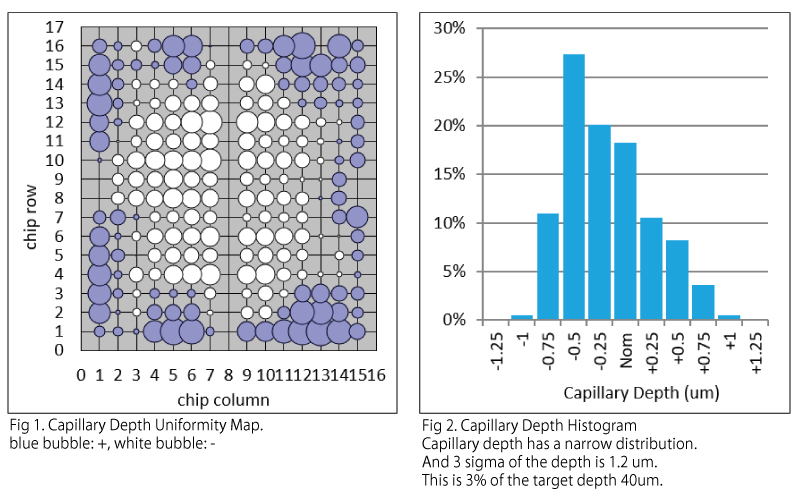
The capillary plates were etched to 40 um depth and 100 um width by dipping type etcher. Oscillation and circulation are controlled to improve uniformity over the whole substrate. Also the composition of HF based etchant is optimized for the glass type. Uniform map (see Fig 1) and uniform distribution of capillary depth was obtained (see Fig 2). The depth of 3sigma was 3% (1.2 um) and the width of 3sigma was 3% (2.5um).
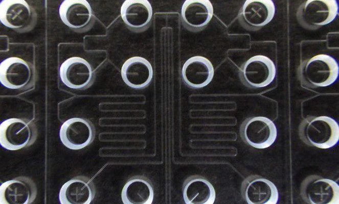
Through-holes were made by micro-blasting method. Dry-film photoresist was used for micro-blasting mask. The blast nozzle scans over whole pattern area and digs holes. When the diameter reaches the target value, micro-blast process was stopped.
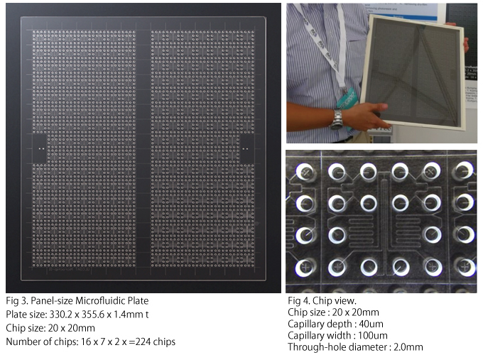
Mask materials were removed from capillary plates and through-hole plates, and both plates were cleaned again. Bonding process was operated under clean benches to reduce particle. Through-holes and etching pattern alignment marks were used to align, and then both plates were bonded temporarily. After temporarily bonding, the plate was baked and permanently bonded. (see Figs 3 and 4)
Fabricating microfluidics chip array on 13 x 14 inch large glass substrates was succeeded. We propose this technology as a solution for High Volume Manufacturing of microfluidics / microstructure devices.
References
[1] “Lead Free Micro Bumping – Cost & Yield Challenges” K. Ruhmer, E. Hughlett, M. Ishizuka, T. Kojima, T. Asaka, B. Dang, A. Buchwalter, D.Shih, EPTC 2007, Singapore, December 2007.
[2] “Fine Pitch Lead Free Solder Bumping with C4NP” K. Ruhmer, E. Laine, M. Ishizuka, T. Kojima, T. Asaka, Semicon Europe Advanced Packaging Conference, Stuttgart, October 2007.

・ULVAC COATING CORPORATION Products
http://www.ulcoat.co.jp/en/product_info/glass/
・Contact Us
http://www.ulcoat.co.jp/en/contact/