ULVAC provides technologies such as ion implanters and sputtering equipment for the manufacturing process of power device IGBTs. Power device IGBT (Insulated Gate Bipolar Transistor) is an acronym for Insulated Gate Bipolar Transistor.
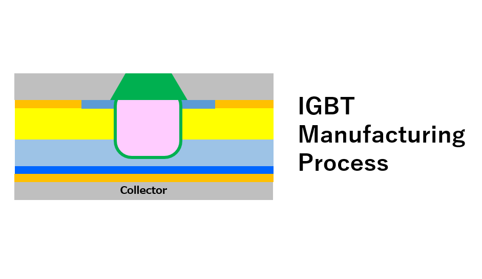
ULVAC provides technologies such as ion implanters and sputtering equipment for the manufacturing process of power device IGBTs. Power device IGBT (Insulated Gate Bipolar Transistor) is an acronym for Insulated Gate Bipolar Transistor.

An optical waveguide is a transmission line that uses light for communication. Quartz-based optical waveguides are basically manufactured using quartz-based glass film deposition technology and etching micromachining technology.
… Waveguide fabrication flow
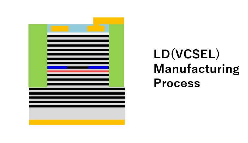
The market for semiconductor lasers is becoming active as a light source for 3D sensing technologies such as LiDAR, which are required for autonomous driving. As one of them, we will introduce a dry process for VCSELs (Vertical Cavity Surface Emitting Laser), which has merits such as miniaturization and energy saving.
… VCSEL fabrication flow

MicroLED is a technology for refining LEDs used as light sources such as lighting and applying them to displays, and is expected as a technology to realize the next generation of displays of liquid crystal and organic EL. ULVAC provides technologies such as ITO sputtering and etching for the MicroLED manufacturing process.
… MicroLED manufacturing

WLP is an abbreviation for Wafer-level Packaging, which is one of the mounting technologies expected as mobile devices such as smartphones become more sophisticated and thinner. ULVAC provides techniques such as sputtering, etching and ashing for the WLP manufacturing process.
… Wafer-level Packaging (WLP) Manufacturing

Infra-red sensor (IR-) is an important sensor for realizing visualization in the dark night, and it can detect the heat of the object, so it can visualize obstacles (animals with a heat source, etc.) even in the dark night.
… Vox(IR sensor) fabrication flow

A SAW device is a filter device that has a structure that excites surface acoustic waves with a thin film of piezoelectric material or a regular comb-shaped electrode formed on a substrate.
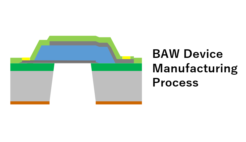
A BAW device is a filter that extracts electrical signals in a specific frequency band by using the bulk vibration of a piezoelectric material.
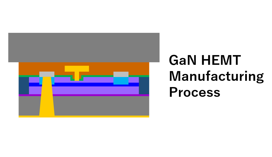
GaN HEMT (High Electron Mobility Transistor) is a next-generation power semiconductor that has low operating resistance and high breakdown withstand voltage, and is expected to be applied to high-power and high-speed electronic devices.
… GaN HEMT fabrication flow
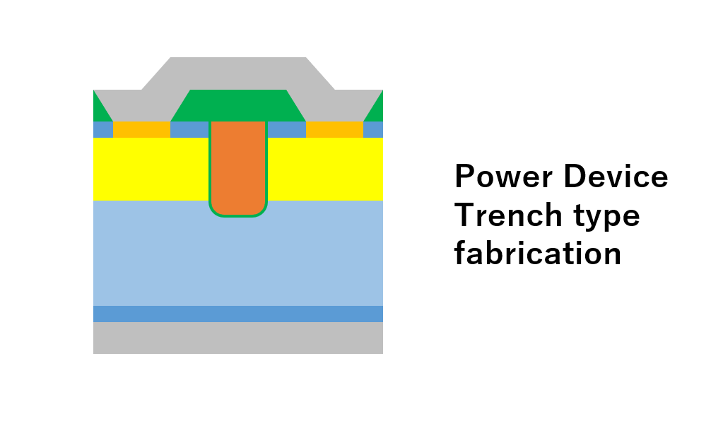
Power devices are expected as devices that achieve low power consumption. Until now, power devices used Si substrates, but due to their limited physical properties, the use of wide bandgap semiconductors such as SiC and GaN is expanding as next-generation substrates. … Trench MOSFET fabrication flow