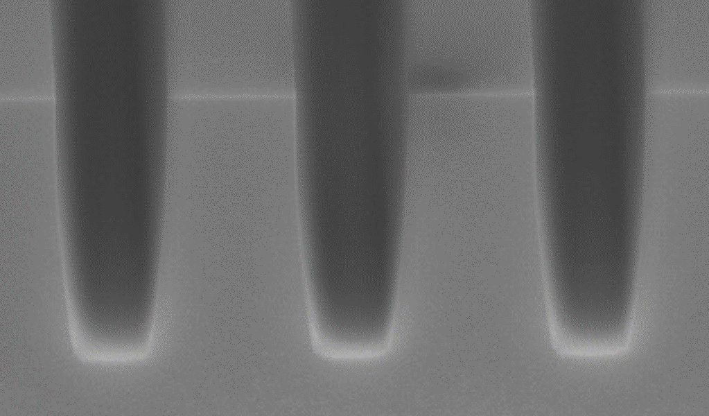
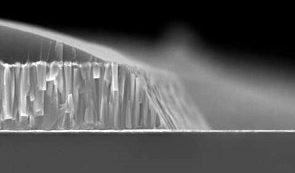
We provide dry etching technology to realize a trench structure that realizes miniaturization and low resistance of power devices.
… SiC Trench etching
We provide dry etching technology to realize a trench structure that realizes miniaturization and low resistance of power devices.
… SiC Trench etching
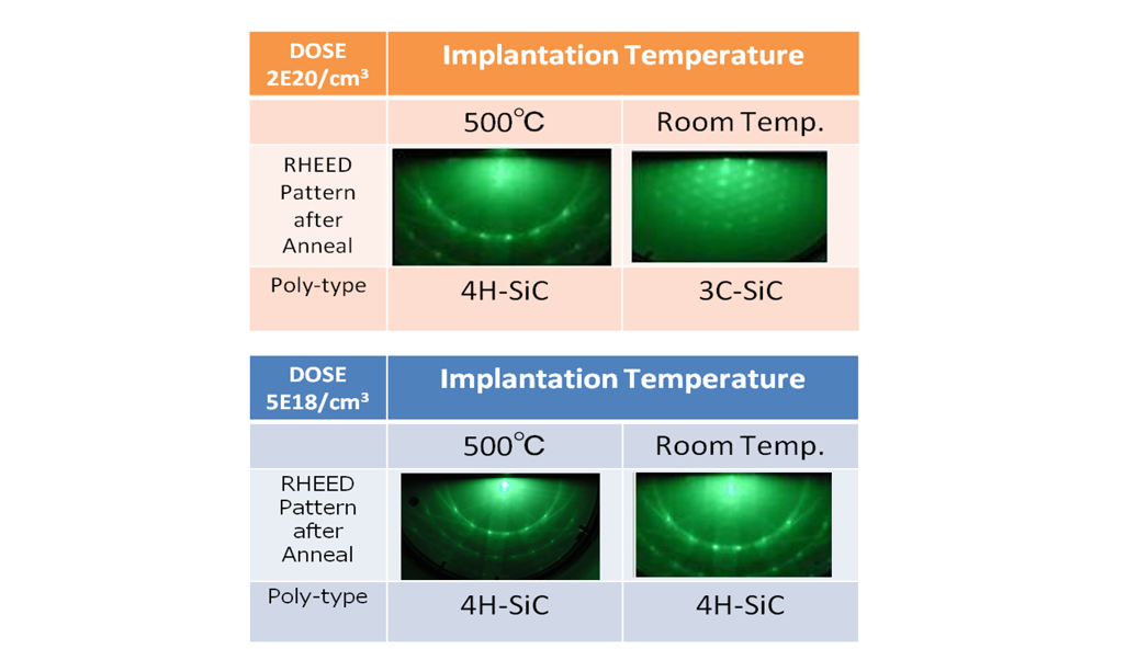
We provide a process that enables high-energy injection and high-temperature and low-temperature injection. We can also provide carbon cap technology that prevents substrate roughness due to Si evaporation during activation annealing.
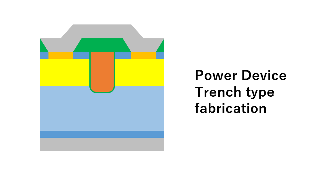
Power devices are expected as devices that achieve low power consumption. Until now, power devices used Si substrates, but due to their limited physical properties, the use of wide bandgap semiconductors such as SiC and GaN is expanding as next-generation substrates. … Trench MOSFET fabrication flow
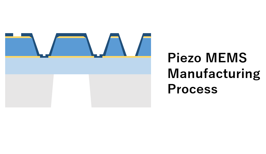
In recent years, MEMS device technology has evolved further and has become indispensable for various sensors and actuators. … Piezoelectric MEMS fabrication flow
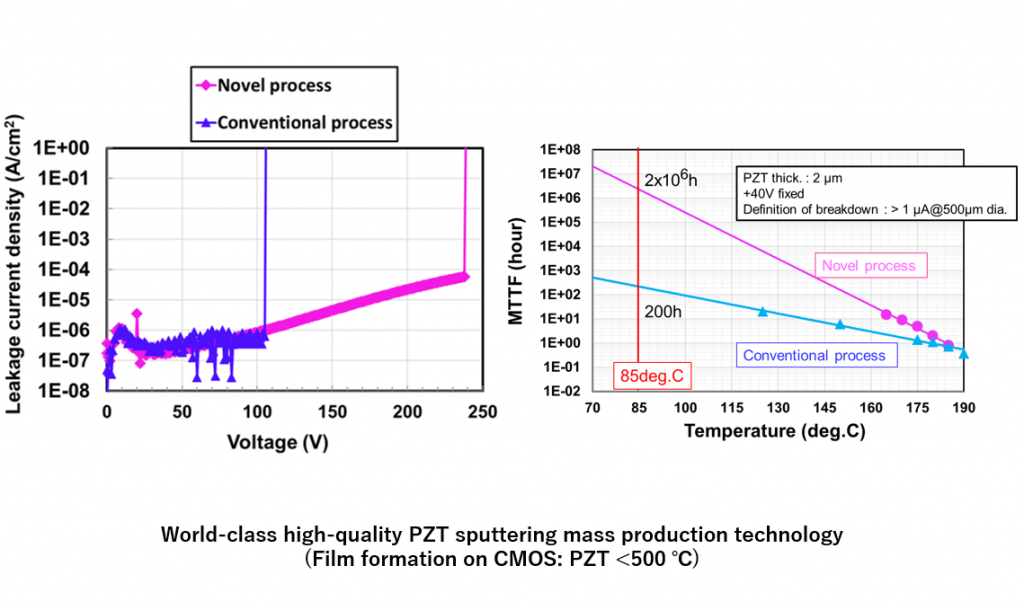
The world’s highest level PZT sputtered film can be stably formed. (Coating on CMOS: PZT film forming temperature <500 ℃)
Equipped with a multi-chamber, PZT full stack (upper and lower electrodes + PZT) can be formed consistently.
We provide Pt / PZT etching process with high selectivity to Pt which is the lower electrode. (Selection ratio: PZT / Pt> 5 @ 8inch,> 10 @ 6inch) It also provides high uniformity (<+/- 3% @ 8inch) that minimizes the amount of underground digging and precise endpoint detection. … PZT film etching for piezoelectric MEMS