In recent years, MEMS device technology has evolved further and has become indispensable for various sensors and actuators. … Piezoelectric MEMS fabrication flow
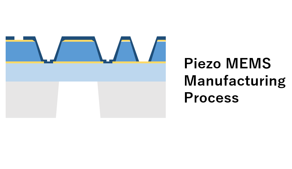
In recent years, MEMS device technology has evolved further and has become indispensable for various sensors and actuators. … Piezoelectric MEMS fabrication flow
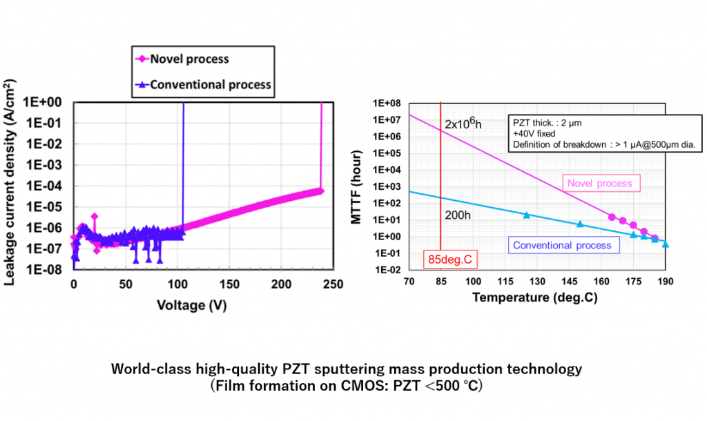
The world’s highest level PZT sputtered film can be stably formed. (Coating on CMOS: PZT film forming temperature <500 ℃)
Equipped with a multi-chamber, PZT full stack (upper and lower electrodes + PZT) can be formed consistently.
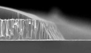
We provide Pt / PZT etching process with high selectivity to Pt which is the lower electrode. (Selection ratio: PZT / Pt> 5 @ 8inch,> 10 @ 6inch) It also provides high uniformity (<+/- 3% @ 8inch) that minimizes the amount of underground digging and precise endpoint detection. … PZT film etching for piezoelectric MEMS